Camera-LCD Interfacing with Microcontroller
 . introduction

CAMERA
 . interpreting vsync/href
 . interpreting pixel values
 . fifo frame buffer
 . sccb/i2c communication

LCD
 . populating with pixels

 . references
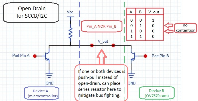
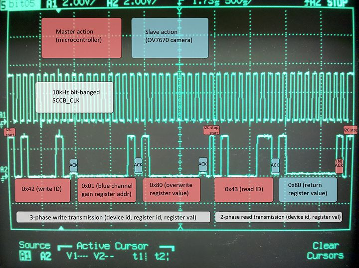
Note how the voltage is slightly above ground when the SCCB slave (camera) outputs a logic 'low' (eg when ACKnowledging or when returning a register value). This is due to the resistor placed on the SCCB data line. Although the resistor is unnecessary for bus fighting prevention since both the SCCB master and slave should be open drain, if the SCCB data signal is measured on the master side of the resistor, the resistor aids in oscilloscope visualization of SCCB communication. That is, the slave will be sinking some current across the resistor, and thus a slave-driven 'low' voltage will appear slightly above ground voltage, an indication that the slave is both alive and talking to the master.
In order to transfer pixels from the camera to the LCD at an 'acceptable' frame rate, a shared 'pixel bus' was created in which a uC, LCD, and camera are all connected together. This allows image pixels to be directly transferred from camera to LCD without being unnecessarily passed through the uC, while at the same time allowing a uC to write pixels to or read pixels from the LCD as desired (eg write to overlay graphics, read to perform image processing operations on pixels). Further, this configuration allows the uC to randomly access pixels from the LCD, which is necessary for image processing algorithms that perform local operations. This is much appreciated, as the camera's FIFO buffer is sequential access and thus does not allow memory reads from arbitrary locations.
Initially, a bit-banged clock was used to transfer the pixels from camera frame buffer to LCD, providing a framerate of 7.5Hz. However, a selectively enabled PWM operating at its maximum frequency of 12MHz was then used as a more autonomous clocking signal. A pulse accumulator is tied to the PWM signal in order to stop the PWM when the appropriate number of pixels have been transferred. A quick calculation shows that the PWM can transfer an entire 'QVGA' frame (313x240) of 2B pixels at (313*240*2) / 12MHz = 12.5ms. This updates the LCD at the 30Hz framerate output by the camera. However, it's clear that as long as the total frame transfer time (pixel clocking + additional housekeeping functions) was below 16.5ms, 60Hz framerate could be achieved.
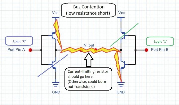
To avoid bus contention over the shared pixel bus and WRITE signal bus, software 'locks' are used to control when relevant uC, LCD, and camera push-pull pins are allowed to be configured as outputs. Consult the following image to understand how push-pull pins are configured as inputs or outputs at the digital circuit level. picture of push-pull output w/ output buffers
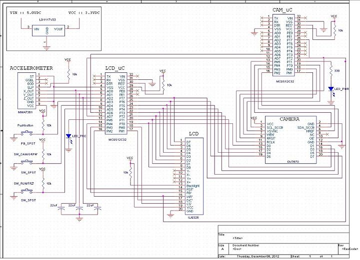
Entire application schematic.
References
[]
[]
[]
[]
